
Advanced Material Characterisation Lab in Gujarat: One Centre for SEM, XRD, AFM, Tribology & Coating
In industrial and research landscape, material performance determines product reliability, safety, and innovation. Whether it is aerospace alloys, semiconductor coatings, battery materials, polymers, or biomedical components, advanced testing and characterisation are essential before deployment. Gujarat is now home to a state-of-the-art Advanced Material Characterisation Lab that integrates SEM, XRD, AFM, Tribology, and coating analysis under one roof, offering a complete micro-to-nano scale evaluation platform.
This high-tech Micro–Nano Research & Development Centre (MNRDC) was established under the Gujarat Industrial Policy 2020 with support from the Industries Commissionerate, Government of Gujarat. The centre focuses on micro- and nano-scale device manufacturing, analysis, and advanced materials research.
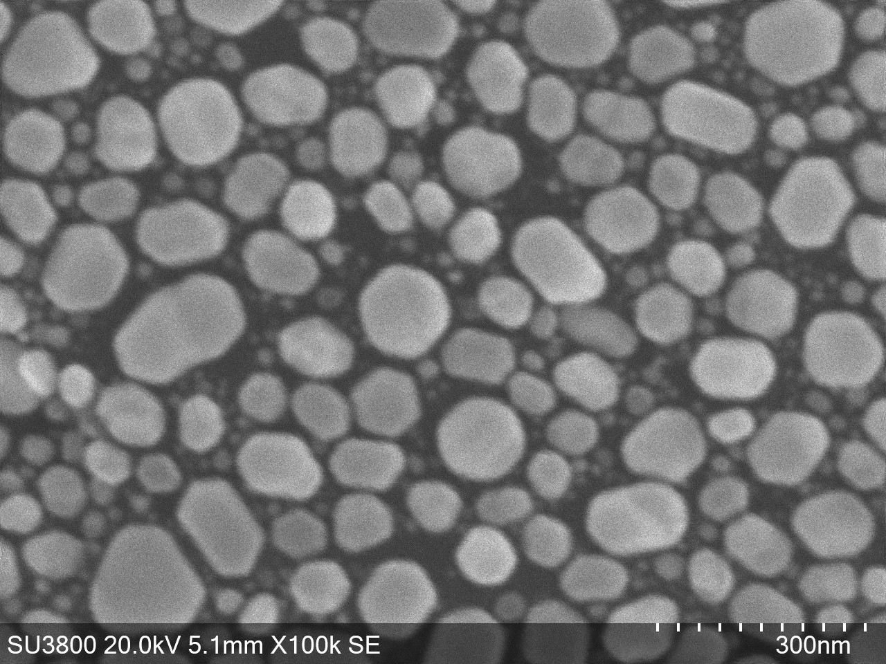
Scanning Electron Microscopy (SEM) with EDS
The lab houses a high-end Scanning Electron Microscope (SEM) integrated with Energy Dispersive Spectroscopy (EDS) system, imported from Japan and valued at ₹1.9 crore. SEM is primarily used for surface morphology analysis, enabling researchers to study:
- Surface structure
- Particle size and distribution
- Micro-cracks and defects
- Coating thickness
- Wear tracks
The SEM operates by generating an electron beam using a tungsten filament, which is focused onto the sample through condenser and objective lenses. It provides high-resolution imaging in micron ranges such as 30 µm, 10 µm, and 5 µm.
The integrated EDS system verifies elemental composition and material purity, making it possible to confirm alloy quality, detect contaminants, and validate powder compositions. Standard output includes 8 SEM images per sample along with EDS spectra, with typical analysis times ranging from 45 to 60 minutes.
X-Ray Diffraction (XRD) – D6 PHASER
While SEM examines surfaces, X-Ray Diffraction (XRD) reveals the internal atomic structure of materials. The lab is equipped with the German-imported D6 PHASER Benchtop XRD system (₹1.06 crore).
XRD works on Bragg’s Law (nλ = 2d sinθ), enabling determination of:
- Crystal structure
- Phase identification
- Residual stress
- Crystallite size
- Material composition
The system uses a CuKα X-ray source and a LYNXEYE XE-T Position Sensitive Detector (PSD) for fast, high-quality scans. Continuous PSD fast mode captures multiple diffraction angles simultaneously, significantly reducing scan time.
The lab utilizes the ICDD PDF-4 reference database, containing over one million diffraction patterns for accurate material identification.
Advanced capabilities include:
- GIXRD (Grazing Incidence XRD) for thin films
- XRR (X-Ray Reflectivity) for coating thickness (1–500 nm), roughness, and density analysis
- TOPAS software with Rietveld refinement for precise quantitative phase analysis
Importantly, XRD is a Non-Destructive Testing (NDT) technique, and samples remain unharmed after testing.
Atomic Force Microscopy (AFM)
For nanoscale surface mapping, the lab features a Core AFM system imported from Switzerland (₹76 lakh). Unlike optical microscopes, AFM “feels” the surface using an ultra-sharp tip (radius 5–10 nm) attached to a cantilever. It works on Hooke’s Law (F = –kx), measuring cantilever deflection to calculate nano-scale forces.
AFM provides:
- Surface roughness measurements
- Step height analysis
- Grain size distribution
- Nano-indentation
- Adhesion and stiffness mapping
Dynamic (tapping) mode is commonly used for precise surface roughness evaluation, especially for optical lenses, semiconductor layers, and nano-coatings. The MountainsSPIP software generates ISO-standard roughness reports and histograms for particle size distribution. AFM can operate in air, liquid, or vacuum environments, expanding its application range.
Pin-on-Disc Tribology Testing
Material durability is validated using the Pin-on-Disc Wear Testing Machine (Tribometer). Operating under ASTM G99 standards, this system evaluates:
- Wear rate
- Coefficient of friction
- Sliding distance
- Surface damage after rubbing
A stationary pin is pressed against a rotating hardened disc under controlled load. Sensors record friction force in real time, generating coefficient-of-friction vs time graphs.
Available test types include:
- Dry wear testing
- Lubricated wear testing
- High-temperature pin heating tests
The software allows comparison of up to six test datasets simultaneously, and detailed Excel reports are provided for further analysis.
Integrated Coating & Surface Analysis Capability
The strength of this advanced lab lies in its integrated testing ecosystem:
- SEM examines coating morphology and wear tracks.
- XRD identifies coating phases and internal stress.
- XRR measures nano-scale thickness and roughness.
- AFM quantifies nanoscale surface smoothness.
- Tribology testing evaluates real-world wear performance.
This unified approach enables complete characterisation, from atomic structure to macro-scale durability.
Industrial & Research Applications
The facility supports industries such as:
- Automotive (brake pads, engine parts, bearings)
- Aerospace (lightweight alloys, wear-resistant coatings)
- Electronics (semiconductor layers, chip surfaces)
- Pharmaceuticals (drug phase identification)
- Energy (battery materials)
- Manufacturing (tool wear and surface treatment validation)
With hundreds of samples already analysed across SEM, XRD, AFM, and tribology platforms, the centre demonstrates strong operational capability.
Conclusion
The Advanced Material Characterisation Lab in Gujarat stands as a comprehensive platform for micro-to-nano scale material evaluation. By integrating SEM, XRD, AFM, tribology, and coating analysis under one roof, it delivers accurate, standards-based, and industry-ready insights. For more details on our specific equipment, visit our Facilities and Services page. In modern engineering and materials science, performance cannot rely on assumptions. With advanced instrumentation, scientific validation ensures that every material, whether metal, polymer, composite, or coating, is thoroughly examined before it meets real-world demands.