
SEM vs XRD vs AFM vs Tribometer – Which Material Characterisation Test Does Your Sample Need?
Complete Decision Guide from Parul University MNRDC. Map your research questions to the right instruments.
Material characterisation is not about running the most tests – it is about running the right test for the question you are asking. Every instrument at the MNRDC answers a different class of questions. Identify which of the following questions your research is asking, and the correct instrument follows directly.
Question 1: What Does the Surface of My Material Look Like?
Answer: SEM + EDS - Hitachi SU3800
Use SEM when you need to see surface morphology – grain structure, particle size and shape, surface defects, fracture patterns, coating uniformity, or phase distribution – at resolutions down to approximately 3-4 nm. Add EDS in the same session to determine elemental composition: which elements are present, in what proportions, and where they are distributed spatially (area mapping).
- Standard output: 8 SEM images + 2 EDS spectra + area mapping on request.
- Turnaround: 10 days standard, 1 day urgent (4 images).
- Sample requirement: Solid (or dried liquid), max 100mm dia × 50mm height.
Question 2: What Crystal Structure Is My Material & Which Phases Does It Contain?
Answer: XRD - Bruker D6 PHASER
Use XRD when you need to identify crystalline phases, measure crystallite size, detect lattice strain, or quantify phase proportions in a mixture. The D6 PHASER uses Bragg’s Law (nλ = 2d sinθ) to generate a unique diffraction fingerprint matched against the ICDD PDF-4 database (1 million+ reference patterns).
- Key Analysis: TOPAS Rietveld refinement for quantitative phase analysis.
- Advanced: GIXRD for thin films; XRR for thickness (1-500nm), roughness, and density.
- Sample requirement: Powder (min 800mg) or solid (max 30mm dia × 5mm thick).
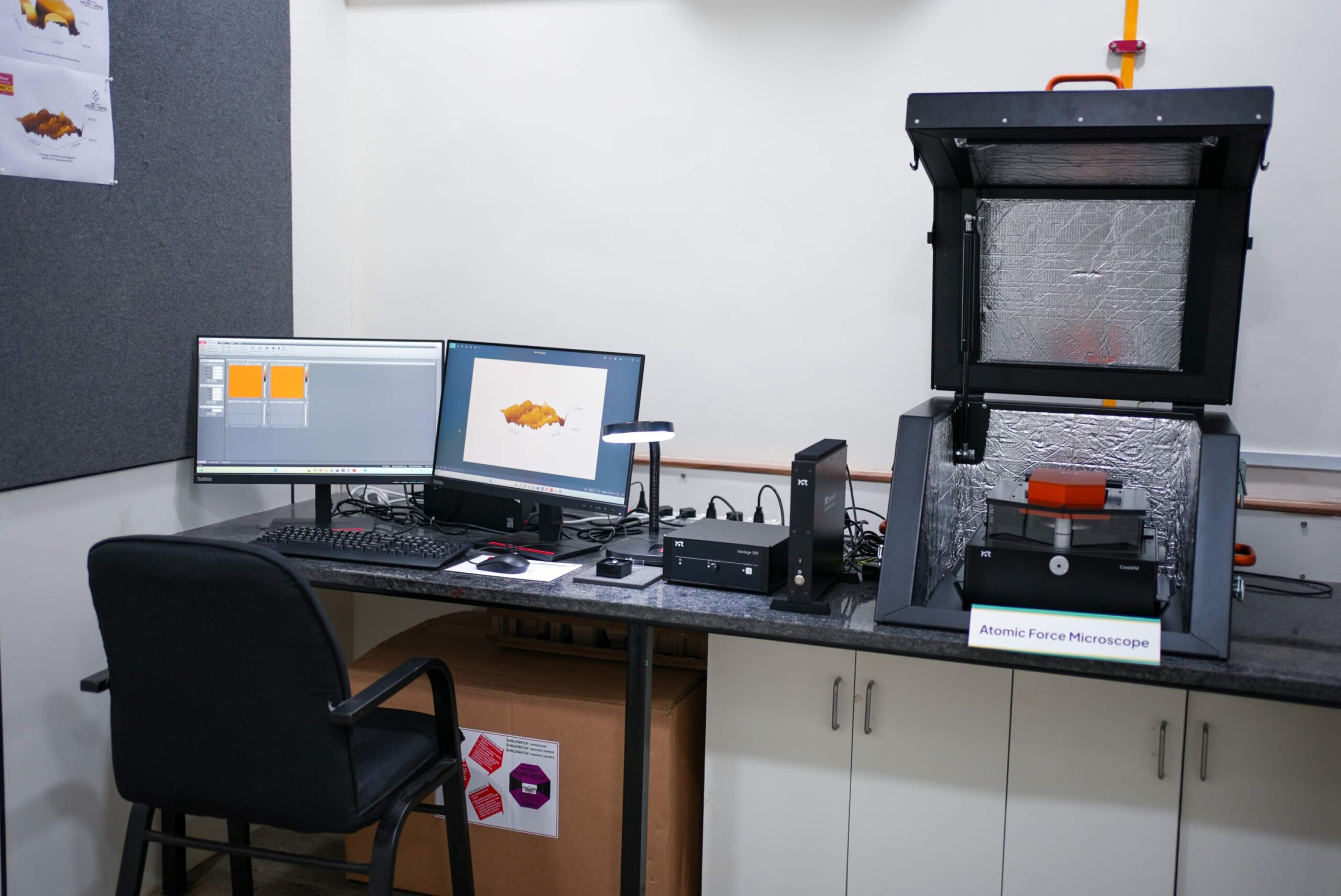
Question 3: How Rough or Smooth Is My Surface at the Nanoscale?
Answer: AFM - Nanosurf Core
Use AFM when you need quantitative nanoscale surface topography – roughness parameters (Ra, Rq, Rz and 50+ ISO S-parameters via MountainsSPIP), 3D surface maps, or grain size at the nanoscale. The Core AFM operates in air, liquid, or vacuum, making it unique for biological sample imaging in physiological conditions.
- Standard output: 2D image, 3D surface render, Excel roughness data, roughness graph.
- Default Mode: Tapping Mode – gentle enough for soft and biological samples.
- Sample requirement: Solid or compacted powder pellet, max 10mm × 10mm × 7mm.
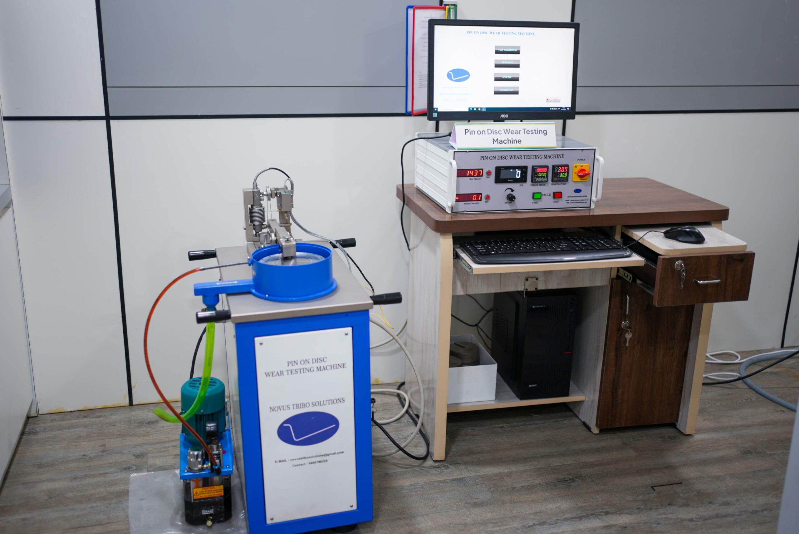
Question 4: How Does My Material Perform Under Friction and Wear?
Answer: Pin-on-Disc Tribometer - NTS-R&D-03
Use the Tribometer when you need wear rate, coefficient of friction (COF), or material durability data under sliding contact. The MNRDC operates to ASTM G99 standard.
- Test Modes: Dry, Lubricated (oil, water, fluid), and Heated (elevated temperature).
- Standard output: Time-resolved friction force, COF, sliding distance, and wear rate.
- Sample requirement: Cylindrical solid pin, 6-12mm diameter, 25-30mm length.
Question 5: What Are the Electrical or Dielectric Properties of My Material?
Answer: LCR Meter ZM2376 - NF Corporation Japan
Use the LCR Meter when you need resistance, capacitance, inductance, impedance, or dielectric permittivity – measured across a frequency sweep from 1 mHz to 5 MHz. High-temperature testing is available up to 1200°C.
- Defining capability: Frequency-dependent characterisation.
- Sample requirement: Solid only (powders as pellets), approx 10-20mm diameter.
Question 6: I Need to Deposit a Thin Film - What Do I Need?
Answer: RF/DC Magnetron Sputtering Auto 500
Use sputtering when you need to coat a substrate with a thin film – metals, oxides, nitrides, or organic compounds – with precise control over thickness and composition.
- Methods: DC sputtering (conductive), RF sputtering (insulators/oxides), and Thermal evaporation.
- Capabilities: Substrate heating to 600°C and rotation for uniform films.
Combination Strategies - Multi-Instrument Workflows
The MNRDC’s integrated portfolio makes multi-instrument workflows practical:
- Pharmaceutical development: XRD (polymorphs) + SEM+EDS (particle shape) + AFM (coating roughness).
- Failure analysis: SEM (fracture morphology) + XRD (phase identity) + Tribometer (wear rate) + EDS (contamination).
- Thin film research: Sputtering (deposition) + XRR (thickness) + GIXRD (crystal structure) + AFM (nanoscale mapping).
- Composite development: Stir Casting (fabrication) + SEM+EDS (distribution) + XRD (phases) + Tribometer (wear resistance).
Quick Reference - Instrument Selection
| Instrument | Primary Use Case |
|---|---|
| SEM + EDS | Surface morphology & elemental composition. |
| XRD | Crystal structure, phase identification, & polymorphism. |
| AFM | Nanoscale roughness & 3D topography. |
| Tribometer | Friction, wear rate, & sliding durability. |
| LCR Meter | Electrical impedance & dielectric permittivity. |
Frequently Asked Questions
What is the difference between SEM and XRD for material characterisation?
SEM images the surface morphology (what it looks like) - including shape, texture, and grain structure. XRD reveals the internal crystal structure (what it is and how it is structured inside). They are complementary: SEM shows appearance, while XRD confirms identity and phase. Both are available at the MNRDC.
When should I use AFM instead of SEM?
Choose AFM when you need quantitative nanoscale roughness parameters (Ra, Rq, Rz), 3D surface topography at nanometre precision, or imaging of non-conductive samples without special coating. Choose SEM for larger-area morphology surveys or when EDS elemental analysis is needed.
Are testing services at Parul University MNRDC non-destructive?
Yes, SEM+EDS, XRD, AFM, and LCR Meter tests are non-destructive, meaning samples remain in their original condition. The Tribometer involves sliding wear and is inherently destructive of the contact surface.
Which test should I use for pharmaceutical particle characterisation?
We recommend using XRD to identify drug polymorphs and confirm crystal structure, combined with SEM+EDS to characterise API particle size and shape. AFM can be used to measure the surface roughness of tablet coatings.