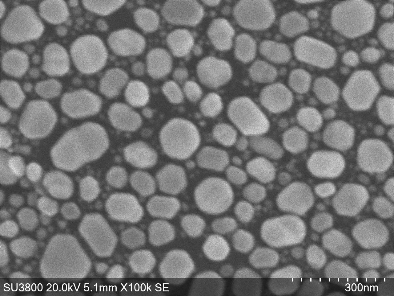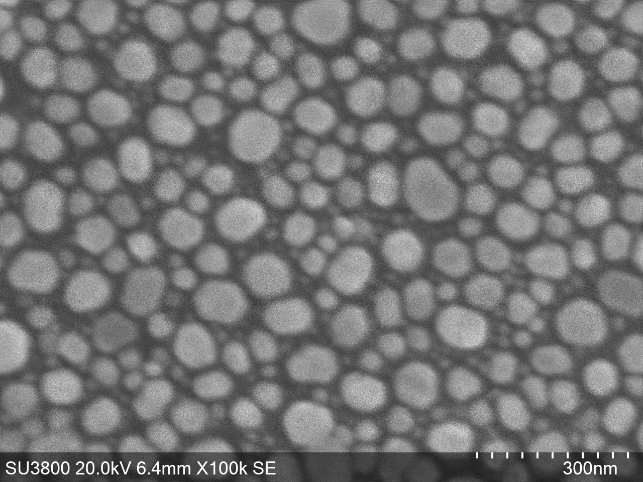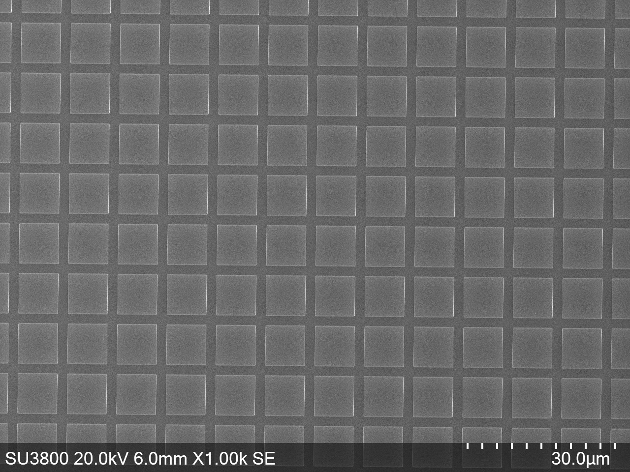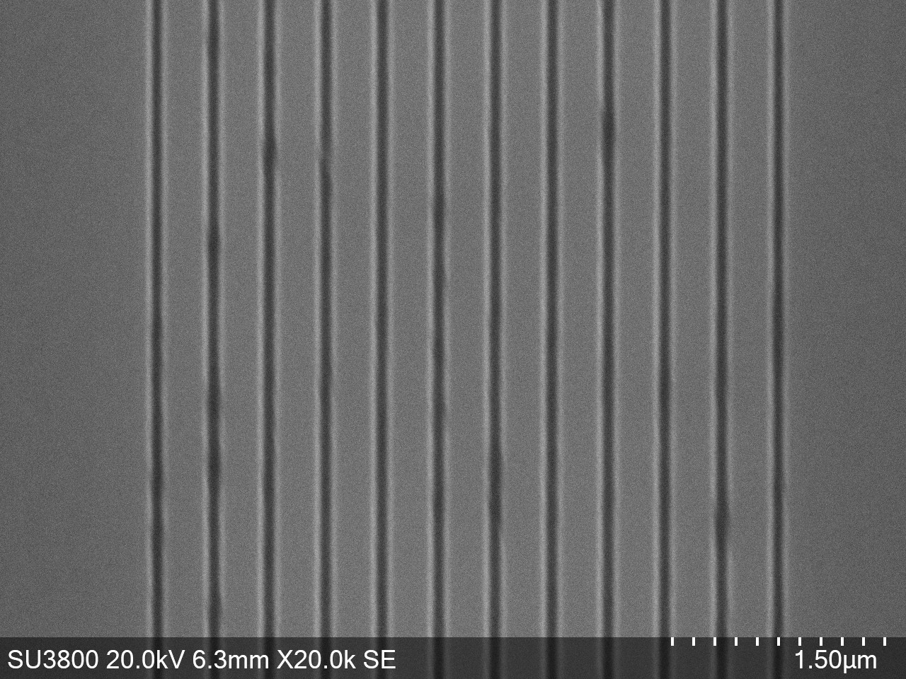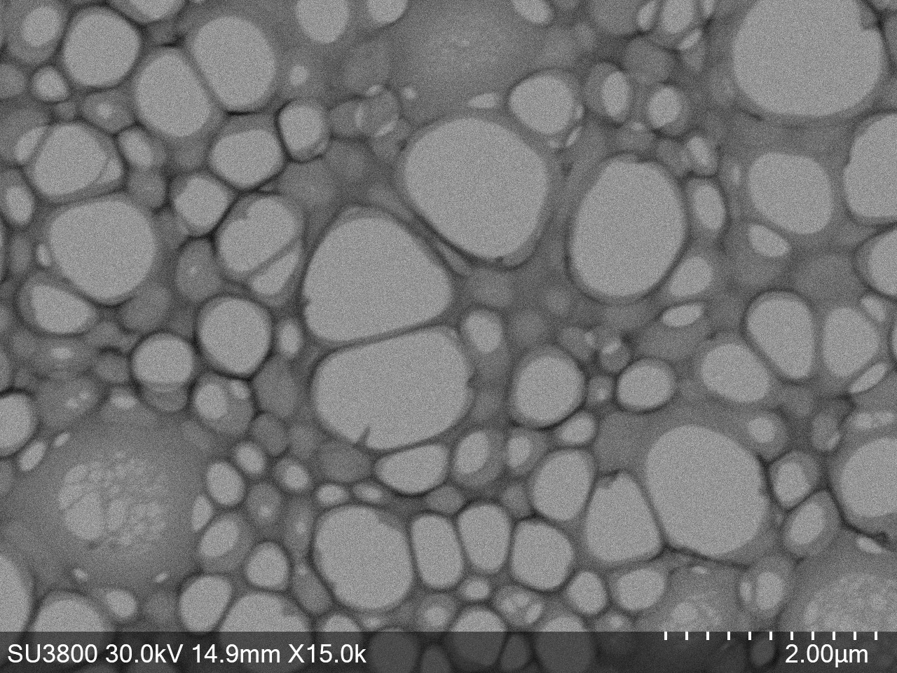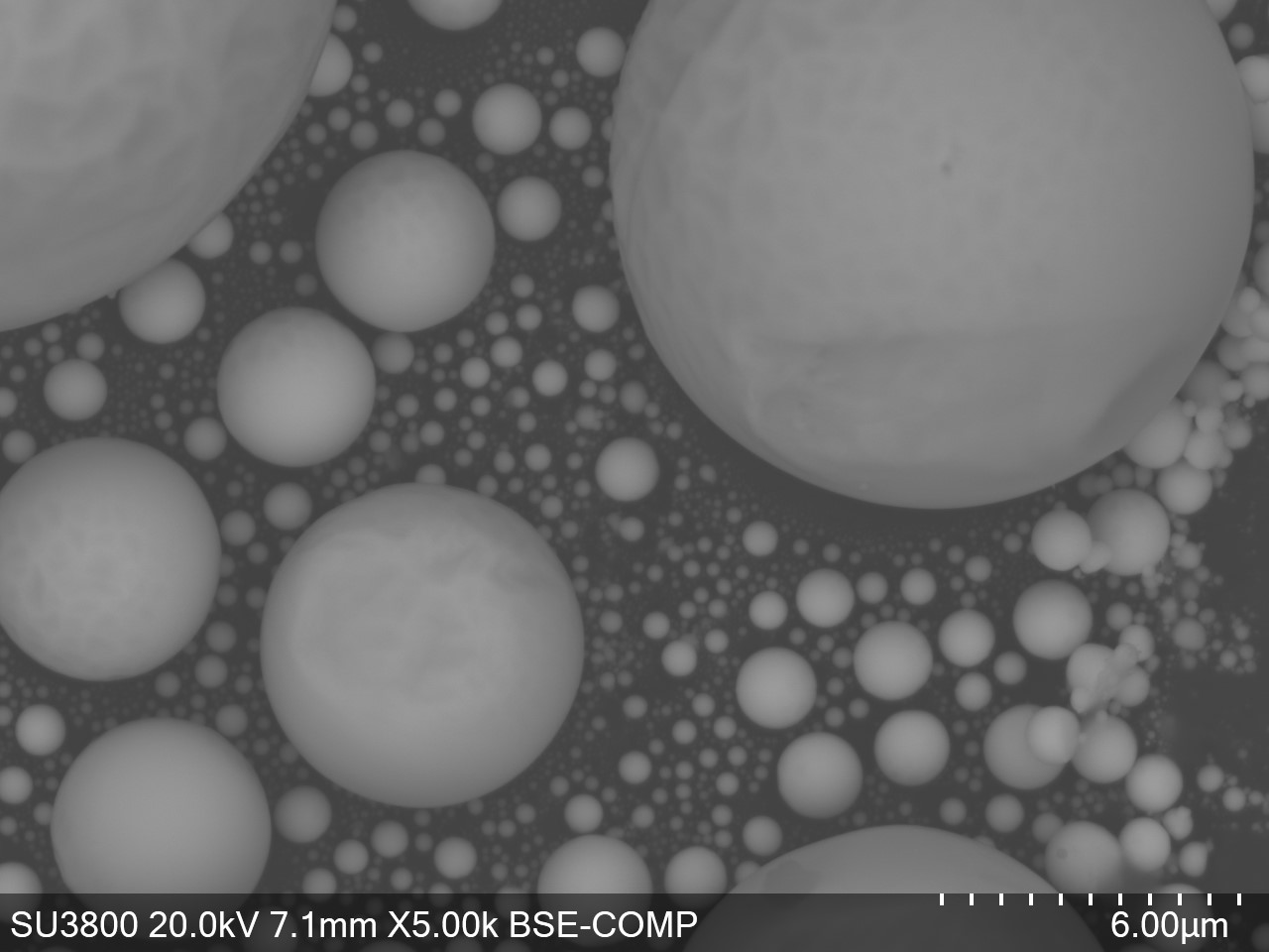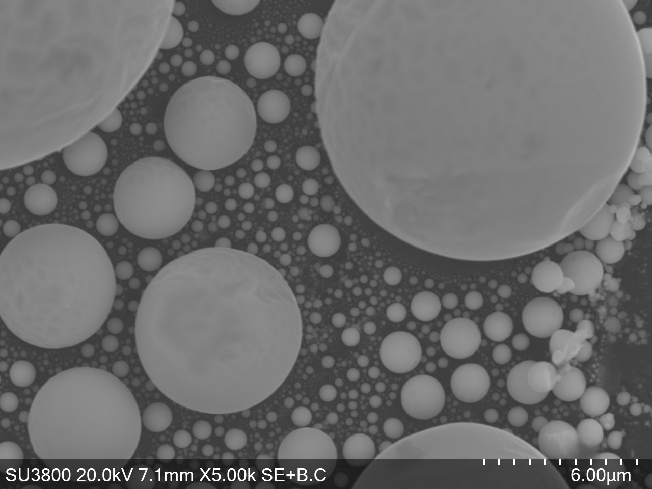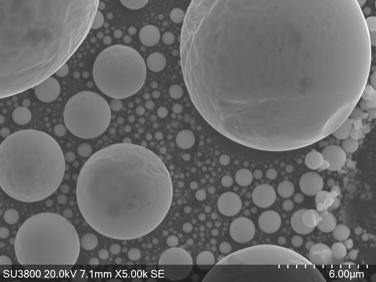
Scanning Electron Microscope (SEM) with EDS
Model Name: SU3800 Hi-SEM with EDS and Sputter Coater
Company Name: Hitachi High-Tech India Pvt. Ltd.
About:
The Hitachi SU3800 SEM performs high-resolution characterization and analysis, yielding precise nanoscale surface information. It is equipped with advanced optics and detection systems, including SE, BSE, UVD, and STEM detectors. The SEM provides comprehensive information about specimen surface morphology, with an EDS system for elemental composition analysis.
Salient Features:
- Five-axis motorized stage with a maximum specimen size of 200mm in diameter.
- High resolution: 3.0 nm at 30kV (High Vacuum Mode) for SE, and 4.0 nm at 30kV (Low Vacuum Mode) for BSE.
- Unique Ultra Variable Pressure Detector (UVD II) for SE imaging and CL imaging.
- Oxford Xplore EDS system for live elemental mapping.
- Gold sputter coating unit for preparing conducting layers on non-conducting samples.
Applications:
- Materials research, nanotechnology, ceramics, composites, polymeric materials, geology, dental materials, biological and soft materials.
